
The Union Budget 2026-27 launched India Semiconductor Mission (ISM) 2.0, and it’s a real shift in direction: instead of just assembly and packaging, India is now aiming at semiconductor equipment, materials, intellectual property, and advanced manufacturing itself.
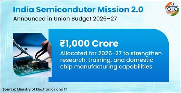
ISM 2.0 gets ₹1,000 crore in FY 2026-27, with most of the weight on industry-led research, innovation, and skill development. The goals are straightforward: build up domestic production, support chip design done in India, and make supply chains harder to disrupt.
Semiconductors sit underneath almost everything now from telecommunications, automobiles, AI, defence, to consumer electronics, healthcare and industrial automation. That’s why building this capability domestically has become both an economic bet and a strategic one.
Where India’s semiconductor market stands
India’s ecosystem has been gaining real momentum, helped along by rising investment, growing manufacturing capacity, and efforts like SEMICON India. Industry estimates put the market at around US$38 billion in 2023, US$45-50 billion in 2024-25, and US$100-110 billion by 2030. It fits the broader Make in India / Make for the World push with India positioning itself as both a place to manufacture and a supplier the world can rely on.
What ISM 1.0 built
The Union Cabinet approved ISM 1.0 in December 2021 with a ₹76,000 crore outlay. It covers up to 50% of project costs for silicon semiconductor fabs, compound facilities, packaging and testing units, and design-linked initiatives.
By December 2025, it had approved 10 projects across six states, totaling ₹1.60 lakh crore investment in silicon fabrication units, silicon carbide fabs, memory and advanced packaging facilities, and assembly and testing infrastructure. Together, these are meant to form a complete domestic semiconductor value chain.
What ISM 2.0 is aiming for
The second phase goes deeper: domestic production of semiconductor equipment and materials, full-stack Indian semiconductor IP, stronger domestic and global supply chains, more advanced manufacturing, and a genuinely skilled workforce.
The target is to be able to design and manufacture chips covering 70-75% of domestic demand by 2029. Longer term, India wants capability at advanced process nodes (3nm and 2nm) and a spot among the world’s leading nations by 2035.
Where the FY27 money is going
The Modified Programme for Development of Semiconductor and Display Manufacturing Ecosystem gets ₹8,000 crore for FY 2026-27, meant to speed up investment and job creation across fabrication, packaging, and design.
One semiconductor fab is planned under the Semiconductor Fabrication Scheme, expected to bring in ₹4,000 crore in investment and create around 1,500 jobs during FY27.
Nine units working on compound semiconductors, silicon photonics, sensors, discrete semiconductors, and ATMP/OSAT facilities are also getting support, projected to bring ₹11,000 crore in investment and 3,000 jobs.
The Design Linked Incentive scheme plans to support 30 design companies in FY27, aiming for 10 new semiconductor IP cores and jobs for 200 design professionals.
Why this matters strategically
Semiconductors now underpin financial systems, telecom networks, energy infrastructure, manufacturing, healthcare, defence, and space technology. COVID-19 made the fragility of this obvious when the global chip shortage disrupted more than 169 industries.
Production is also heavily concentrated: Taiwan makes more than 60% of the world’s semiconductors and close to 90% of advanced chips. That concentration is exactly why countries everywhere, India included, are racing to build domestic capacity not to cut themselves off from global supply chains, but to have real standing within them.
Design ecosystem progress
The Design Linked Incentive Scheme, running since 2021, has become one of the pillars of India’s semiconductor strategy. As of January 2026, it’s supporting 24 design startups, which have pulled in nearly ₹430 crore in venture funding. The national chip design platform has logged about 2.25 crore Electronic Design Automation tool hours, with around 67,000 students and 1,000 startup engineers actively using the tools.
Academic institutions have taped out 122 chip designs, with 56 chips fabricated at the Semiconductor Laboratory in Mohali using 180nm technology. Startups have completed 16 tape-outs, six of which were fabricated at foundry nodes as advanced as 12nm. On the patent side, academic institutions have filed 75 and startups 10. The next phase is targeting at least 50 fabless semiconductor companies.
Homegrown processors
India has also been building its own processor technology. The latest milestone is DHRUV64, a fully indigenous 64-bit microprocessor developed by the Centre for Development of Advanced Computing, aimed at 5G infrastructure, automotive electronics, industrial automation, consumer devices, and IoT.
DHRUV64 joins a growing lineup that includes SHAKTI, AJIT, VIKRAM, and THEJAS, all developed under the Digital India RISC-V Programme, which uses open-source RISC-V architecture specifically to cut licensing costs and open the field up to more innovation.
Building the talent pipeline
Infrastructure alone doesn’t make an ecosystem, so several skilling programmes are running alongside the manufacturing push.
The Chips to Startup Programme gives 397 universities and startups access to advanced chip design tools. Researchers from more than 46 universities have already designed and fabricated 56 chips at the Mohali lab.
AICTE has introduced new academic tracks: B.Tech programmes in VLSI and semiconductor engineering, diploma courses in IC manufacturing, and minor degrees in semiconductor technologies.
The SMART Lab at NIELIT Calicut is aiming to train one lakh engineers in semiconductor technologies more than 62,000 have already finished training. A partnership with Lam Research is targeting 60,000 professionals trained in nanofabrication and advanced packaging over the next decade. FutureSkills PRIME rounds this out with industry-aligned digital learning modules covering semiconductors and other emerging technologies.
Key Takeaway: ISM 2.0 marks a shift from simply building the ecosystem to deepening it stronger manufacturing, real design capability, homegrown IP, and a trained workforce all moving together. Between the rising investment, the growing design base, and a clear roadmap toward advanced process nodes, India is making a genuine push to become a serious global centre for semiconductor design, manufacturing, and innovation.
MCQ:
1. India Semiconductor Mission (ISM) 1.0 was approved by the Union Cabinet in which year?
A. 2019
B. 2020
C. 2021
D. 2022
2. The indigenous 64-bit microprocessor DHRUV64 has been developed by which organisation?
A. ISRO
B. DRDO
C. Centre for Development of Advanced Computing (C-DAC)
D. Bharat Electronics Limited (BEL)
Read more: SEED Scheme Benefits and Beneficiaries – Education, Livelihood & Healthcare