

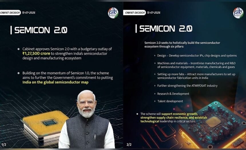
The Union Cabinet, led by PM Narendra Modi, has cleared Semicon 2.0, a ₹1,27,500 crore programme aimed at building out India’s semiconductor design and manufacturing base. It picks up where Semicon 1.0 left off, with a focus on long-term policy backing, stronger domestic capabilities, and turning India into a serious player in global chip innovation and production.
Six pillars
The programme rests on six pillars covering different parts of the semiconductor value chain.
Chip design comes first. There are already 105 startups working in this space, and the goal now is to build out IP, chip designs and system-level solutions for both strategic and commercial use, with India positioning itself as a design IP hub.
The second pillar covers semiconductor equipment, materials, chemicals and gases. Companies working in these areas will get incentives to build a domestic supply chain and sharpen precision manufacturing.
Third comes fabrication plants, silicon fabs, compound semiconductor fabs, discrete component fabs and display fabs. India’s first fab is expected to come online in 2028, and the government wants more global manufacturers setting up shop here.
The fourth pillar targets ATMP and OSAT, assembly, testing, marking, packaging and outsourced assembly and test, with an eye on advanced packaging tech and making India an alternative to existing global manufacturing hubs.
Fifth is R&D, pushing beyond current 28nm-110nm nodes through partnerships with research institutions in India and elsewhere.
The sixth pillar is talent. 315 universities are already teaching chip design using EDA tools, and about 68,000 students have been trained so far. The plan is to expand this further into clean-room operations, fab construction and other specialised skills, working alongside industry.
Beyond the semiconductor sector itself, the government expects the programme to feed into broader economic growth, tighten supply chain security, and build up India’s standing in strategic tech industries.
Key Takeaway: Under the first phase, the government approved 12 semiconductor manufacturing units, totalling over ₹1.64 lakh crore in investment. That includes one silicon fab, one silicon carbide fab, one integrated gallium nitride Micro LED display fab, and nine packaging units, spanning consumer electronics, industrial electronics, automobiles, power electronics, telecom and aerospace. Micron, Kaynes and CG Semi are already in commercial production, with one more unit expected to start in 2026.
On design, 24 startup and MSME projects have been approved for financial support, and 105 startups and MSMEs now have access to industry-standard EDA tools. They’re building chips and SoC solutions for satellite communications, drones, surveillance, IoT, LED drivers, AI, telecom equipment and smart meters, with some projects already moving toward prototyping and deployment.
With Semicon 2.0, the government is putting ₹1.27 lakh crore behind the next stage: design, manufacturing, research, packaging and talent, building on what Semicon 1.0 has already delivered.
MCQ’s:
1. How many universities are currently teaching chip design using EDA tools under the semiconductor ecosystem?
A. 105
B. 210
C. 315
D. 500
2. Approximately how many students have already been trained in chip design-related skills?
A. 24,000
B. 50,000
C. 68,000
D. 1,05,000
Read more: Revolutionary Ultra-Sensitive Ammonia Sensor – Wearable Gas Detection Devices